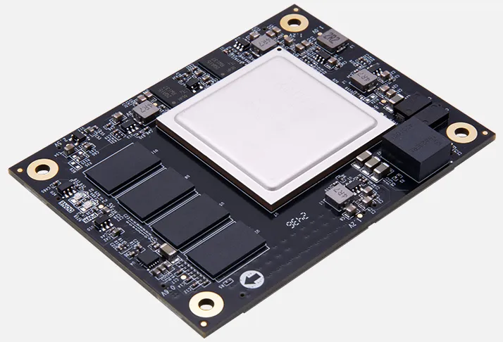
Description and Technical Data:
1) Overview/Key Features
The ACKU040 is a high-performance FPGA System-on-Module based on the Kintex UltraScale XCKU040 FPGA. It integrates high-speed DDR4 memory, Quad-SPI Flash, PCI Express connectivity, and multiple high-speed GTH transceivers in an 80 × 60 mm pluggable module. The module is suited to demanding applications such as data-center acceleration, storage acceleration, industrial and scientific systems, medical imaging, machine vision, wired and wireless communications, optical transport, radio, and baseband processing.
- Kintex UltraScale XCKU040 FPGA using 20 nm technology
- Up to 1.5 million system logic units
- Up to 8.2 TeraMAC DSP performance
- 4 GB 64-bit DDR4 SDRAM
- 2 × 16 MB Quad-SPI Flash
- PCIe Gen3 ×8 interface
- 20 × GTH gigabit transceivers with speeds up to 16.3 Gbps
- 99 HR FPGA I/Os and 255 HP FPGA I/Os
- 6 × board-to-board connectors
- 12 V single-supply operation
- -40°C to +85°C operating temperature range
- 80 × 60 mm module size
NCNR non cancelable - non returnable product. B2B customers please contact Mirifica Industrial for volume quotes. Mirifica Industrial ships world-wide.
2) Tech Specs
| Specification | Detail |
|---|---|
| FPGA device | XCKU040-2FFVB1156I |
| FPGA family | Kintex UltraScale |
| Process technology | 20 nm |
| System logic capacity | Up to 1.5 million system logic units |
| DSP performance | Up to 8.2 TeraMAC |
| DDR4 SDRAM | 4 GB, 64-bit |
| Quad-SPI Flash | 2 × 16 MB |
| PCI Express | PCIe Gen3 ×8 |
| GTH transceivers | 20, supporting speeds up to 16.3 Gbps |
| HR FPGA I/Os | 99 |
| HP FPGA I/Os | 255 |
| Board-to-board connectors | 6 |
| Input power | 12 V single supply |
| Operating temperature | -40°C to +85°C |
| Dimensions | 80 × 60 mm |
3) Tech Support/Dokuments
Web available technical information usually covers the ACKU040 FPGA device, memory resources, high-speed transceivers, PCIe interface, FPGA I/O resources, electrical requirements, operating temperature, module dimensions, and application areas. There are the following technical resources listed under the product documentation area:
- ACKU040 V2.0 User Manual
- ACKU040 V3.0 User Manual
Contact Mirifica Industrial for further detailed information for your project.
4) Related Product Suggestion
- AXKU040 FPGA Development Board & Kit
- AXKU041 FPGA Development Board & Kit
- AXKU042 FPGA Development Board & Kit
- ACKU060 FPGA System-on-Module
- ACKU095 FPGA System-on-Module
5) Downloads/Links
6) What is in the package
The package contains.
- 1 x ACKU040 FPGA System-on-Module
More Details:
FPGA Modules