Description and Technical Data:
1) Overview/Key Features
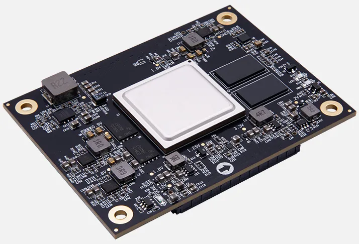
The ACKU5 is an industrial-grade Kintex UltraScale+ FPGA system-on-module based on the XCKU5P-2FFVB676I device. It combines high-density FPGA logic, DDR4 memory, QSPI Flash, high-speed GTY transceivers, PCIe Gen3 connectivity, and 100G Ethernet capability in a compact module format.
The module is suitable for packet processing, digital signal processing, wireless MIMO, high-speed wired networking, data-center networking and storage acceleration, video image processing, industrial control, machine vision, Internet of Things, and medical imaging.
Key features include:
- XCKU5P-2FFVB676I Kintex UltraScale+ FPGA
- 2 GB DDR4 SDRAM with a 32-bit bus
- 64 MB QSPI Flash
- 16 x GTY transceivers with data rates up to 28.21 Gbps
- PCIe Gen3 x16 capability
- 100G Ethernet support
- 179 configurable FPGA I/Os
- 72 HD I/Os
- 96 HP I/Os
- 45 LVDS pairs
- 2 x 240-pin Samtec board-to-board connectors
- 2 x 200 MHz differential crystal oscillators
- 3 x LEDs
- 12 V DC power supplied through the board-to-board connector
- 80 mm x 60 mm x 9.6 mm module dimensions
- 14-layer PCB with independent ground and power layers
NCNR non cancelable - non returnable product. B2B customers please contact Mirifica Industrial for volume quotes. Mirifica Industrial ships world-wide.
2) Tech Specs
| Specification | Detail |
|---|---|
| FPGA device | XCKU5P-2FFVB676I |
| FPGA family | Kintex UltraScale+ |
| Speed grade | -2 |
| Temperature range | -40 °C to +85 °C |
| System logic cells | 475 K |
| CLB flip-flops | 434 K |
| CLB LUTs | 217 K |
| Maximum distributed RAM | 6.1 Mb |
| Total block RAM | 16.9 Mb |
| UltraRAM | 18.0 Mb |
| Clock management tiles | 4 |
| DSP slices | 1,824 |
| GTY transceivers | 16 x, up to 28.21 Gbps |
| PCI Express | PCIe Gen3 x16 |
| 100G Ethernet | 1 x, with KR4 RS-FEC |
| DDR4 SDRAM | 2 GB, 32-bit bus, up to 2666 Mbps |
| QSPI Flash | 64 MB, using 2 x 32 MB devices |
| FPGA user I/Os | 179 total |
| HD I/Os | 72 |
| HP I/Os | 96 |
| LVDS pairs | 45 |
| Board-to-board connectors | 2 x 240-pin high-speed connectors |
| Clock sources | 2 x 200 MHz differential crystal oscillators |
| LEDs | 3 x: power, configuration, and user |
| Power input | 12 V DC through the board-to-board connector |
| Module dimensions | 80 mm x 60 mm x 9.6 mm |
| PCB construction | 14-layer PCB with independent ground and power layers |
3) Tech Support/Documents
Web available technical information usually covers the XCKU5P FPGA, FPGA logic resources, DDR4 memory, QSPI Flash, GTY transceivers, PCIe Gen3, 100G Ethernet, FPGA I/O, board-to-board connectors, clock sources, LEDs, power input, PCB construction, module dimensions, and compatible carrier-board operation. There are the following technical resources available: user documentation, technical specifications, schematics, pin assignments, tutorials, and demonstration projects.
Contact Mirifica Industrial for further detailed information for your project.
4) Related Product Suggestion
The corresponding AXKU5 development board is identified as a compatible carrier board for the ACKU5 system-on-module.
5) Downloads/Links
6) What is in the package
The package contains.
- 1 x FPGA system-on-module
- 1 x DC fan, optional
More Details:
FPGA Modules