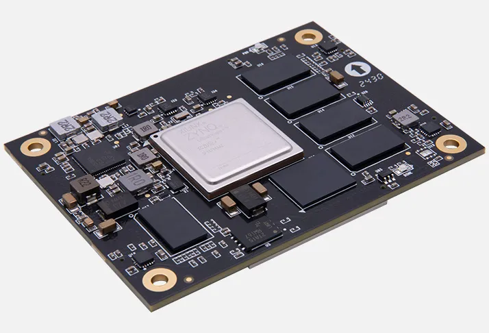
Description and Technical Data:
1) Overview/Key Features
The ACU5EV is a high-end Zynq UltraScale+ MPSoC EV system-on-module based on the XCZU5EV-2SFVC784I device. It combines quad-core application processing, dual-core real-time processing, programmable logic, video-processing capability, DDR4 memory, flash storage, and high-speed interfaces for industrial, multimedia, embedded-vision, 5G, and advanced driver-assistance applications.
- XCZU5EV-2SFVC784I industrial-grade MPSoC.
- 4 x Arm Cortex-A53 processors operating at up to 1.333GHz.
- 2 x Arm Cortex-R5 processors operating at up to 533MHz.
- Arm Mali-400 MP2 GPU.
- H.264/H.265 video codec.
- 4GB PS DDR4 memory with a 64-bit bus.
- 1GB PL DDR4 memory with a 16-bit bus.
- 8GB eMMC Flash.
- 256Mbit QSPI Flash.
- 16 GTH transceivers with data rates up to 16.3Gb/s.
- 4 rear-side 120-pin I/O connectors.
- PCIe, USB 3.0, SATA, DisplayPort, Ethernet, CAN, UART, I2C, SPI, GPIO, and SD/SDIO interfaces.
- 80mm x 60mm module size.
- Operating temperature range from -40°C to 85°C.
NCNR non cancelable - non returnable product. B2B customers please contact Mirifica Industrial for volume quotes. Mirifica Industrial ships world-wide.
2) Tech Specs
| Specification | Detail |
|---|---|
| Module type | Zynq UltraScale+ MPSoC EV system-on-module |
| MPSoC device | XCZU5EV-2SFVC784I |
| Application processors | 4 x Arm Cortex-A53, up to 1.333GHz |
| Real-time processors | 2 x Arm Cortex-R5, up to 533MHz |
| GPU | Arm Mali-400 MP2 |
| Video codec | H.264/H.265 |
| PS DDR4 memory | 4GB, 64-bit bus, 2400Mbps |
| PL DDR4 memory | 1GB, 16-bit bus, 2400Mbps |
| eMMC Flash | 8GB |
| QSPI Flash | 1 x 256Mbit |
| PCIe | PCIe Gen2 x4 |
| USB 3.0 | 2 channels |
| SATA | SATA 3.1 |
| DisplayPort | DisplayPort interface |
| Ethernet | 4 x tri-mode Gigabit Ethernet |
| General connectivity | 2 x USB 2.0, 2 x SD/SDIO, 2 x UART, 2 x CAN 2.0B, 2 x I2C, 2 x SPI, and 4 x 32-bit GPIO |
| GTH transceivers | 16 x 16.3Gb/s transceivers |
| Logic cells | 256K |
| CLB flip-flops | 234K |
| CLB look-up tables | 117K |
| Maximum distributed RAM | 3.5Mb |
| Total block RAM | 5.1Mb |
| UltraRAM | 18.0Mb |
| Clock management tiles | 4 |
| DSP slices | 1,248 |
| 1.8V high-performance I/O | 96 |
| 3.3V high-density I/O | 84 |
| Operating temperature | -40°C to 85°C |
| Module dimensions | 80mm x 60mm |
| PCB | 16-layer immersion-gold PCB with independent ground and power layers |
GitHub1
3) Tech Support/Documents
Web available technical information usually covers the ACU5EV system-on-module overview, MPSoC resources, processor configuration, memory architecture, high-speed interfaces, general connectivity, transceivers, module dimensions, and electrical operating conditions. There are the following technical resources:
- ACU5EV user manual.
- ACU5EV schematic.
- ACU5EV system-on-module reference design.
- ACU5EV 3D STEP model.
- ACU5EV CE compliance information.
- Development information for the AXU5EV-E carrier board.
- Development information for the AXU5EV-P PCIe development board.
Contact Mirifica Industrial for further detailed information for your project.
4) Related Product Suggestion
- AXU5EV-E carrier board.
- AXU5EV-P PCIe development board with SFP+ and FMC interfaces.
GitHub1
5) Downloads/Links
6) What is in the package
The package contains.
- 1 x ACU5EV FPGA board
More Details:
SoC Modules