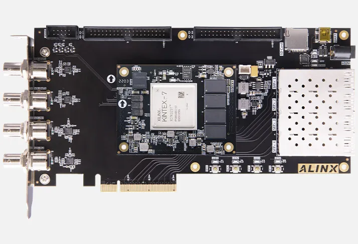
Description and Technical Data:
1) Overview/Key Features
The AV7K300 is a high-performance Kintex-7 FPGA development board designed for video processing, serial digital interface applications, fiber-optic communication, wireless research, and industrial applications. It combines an XC7K325T FPGA system-on-module with a carrier board featuring 3G-SDI, SFP+, PCIe, memory, expansion, and debugging interfaces.
Key features include:
- XC7K325T-2FFG900I Kintex-7 FPGA
- 2 GB DDR3 SDRAM with a 64-bit bus
- 128 Mbit QSPI Flash
- 4 x 3G-SDI interfaces
- 2 x 3G-SDI inputs and 2 x 3G-SDI outputs
- 4 x SFP+ interfaces
- 1 x PCIe Gen2 x8 interface
- 16 x GTX transceivers with data rates up to 12.5 Gbps
- 1 x 12-bit, 1 Mbps analog-to-digital converter
- 2 x 40-pin expansion ports
- 1 x MicroSD card slot
- 1 x USB-UART interface
- 1 x standard JTAG interface
- 2 x active differential clock sources
- 2 x LEDs on the system-on-module board
- 7 x LEDs on the carrier board
- 4 x user keys
- 12 V DC power input
- 215 mm x 111 mm carrier board
- 80 mm x 60 mm system-on-module
NCNR non cancelable - non returnable product. B2B customers please contact Mirifica Industrial for volume quotes. Mirifica Industrial ships world-wide.
2) Tech Specs
| Specification | Detail |
|---|---|
| FPGA device | XC7K325T-2FFG900I |
| FPGA family | Kintex-7 |
| Speed grade | -2 |
| Temperature grade | Industrial grade |
| Logic cells | 326,080 |
| CLB flip-flops | 407,600 |
| Look-up tables | 50,950 |
| Block RAM/FIFO with ECC | 445 blocks, 36 Kb each |
| Total block RAM | 16,020 Kb |
| Maximum distributed RAM | 4,000 Kb |
| DSP48 slices | 840 |
| GTX transceivers | 16, up to 12.5 Gbps |
| PCI Express | PCIe Gen2 x8 |
| DDR3 SDRAM | 4 x 512 MB devices, 2 GB total, 64-bit bus |
| DDR3 data rate | 1600 Mbps |
| QSPI Flash | 128 Mbit |
| 3G-SDI interfaces | 4 x interfaces: 2 x input and 2 x output |
| SFP+ interfaces | 4 x, up to 10 Gbps per channel |
| Analog-to-digital converter | 1 x 12-bit, 1 Mbps |
| Expansion ports | 2 x 40-pin, 2.54 mm pitch, each with 34 I/O connections |
| USB-UART | 1 x interface for serial communication |
| JTAG | 1 x 10-pin, 2.54 mm standard interface |
| Clock sources | 200 MHz PS clock and 125 MHz GTX transceiver clock |
| MicroSD card slot | 1 x, supporting SD mode and SPI mode |
| LEDs | 2 x on the system-on-module board and 7 x on the carrier board |
| User keys | 4 x |
| Power input | 12 V DC, maximum 3 A, 2.1 mm x 5.5 mm connector |
| Carrier board dimensions | 215 mm x 111 mm |
| System-on-module dimensions | 80 mm x 60 mm |
| Carrier board PCB | 6-layer board with independent ground and power layers |
| System-on-module PCB | 14-layer board with independent ground and power layers |
3) Tech Support/Documents
Web available technical information usually covers the AC7K325B system-on-module, the Kintex-7 FPGA, DDR3 memory, QSPI Flash, FPGA resources, GTX transceivers, PCIe, 3G-SDI, SFP+, analog-to-digital conversion, clock sources, JTAG, USB-UART, MicroSD, expansion ports, LEDs, keys, power requirements, PCB construction, and board dimensions. There are the following technical resources available: user manuals, board specifications, pin assignments, schematics, tutorials, and demonstration projects.
Contact Mirifica Industrial for further detailed information for your project.
4) Related Product Suggestion
The manufacturer’s product information identifies the following compatible expansion applications for the 40-pin expansion ports:
- Binocular camera module
- TFT LCD screen
- Camera module
- AD/DA module
5) Downloads/Links
6) What is in the package
The package contains.
- 1 x FPGA board
- 1 x installed DC fan
- 1 x Mini-USB cable
- 1 x programming cable set
- 1 x 12 V power adapter
- 1 x PCIe fence
More Details:
FPGA Dev Boards