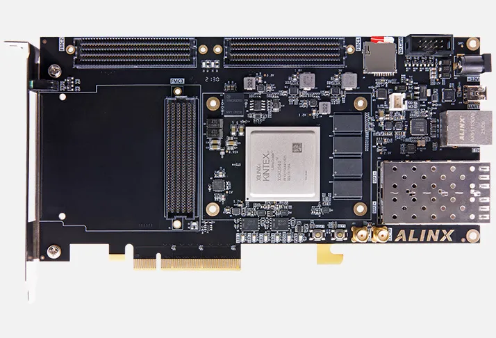
Description and Technical Data:
1) Overview/Key Features
The AXKU041 is a Kintex UltraScale FPGA development board based on the XCKU040-2FFVA1156I FPGA. It is designed for high-speed data exchange, packet processing, DSP-intensive applications, medical imaging, 8K/4K video processing, and heterogeneous wireless infrastructure.
The board provides PCI Express Gen3 x8 connectivity, 2 x 10G SFP+ interfaces, 3 FMC expansion ports, 4 GB DDR4 memory, 64 MB QSPI Flash, Gigabit Ethernet, high-speed SMA interfaces, and a Micro SD card interface. It can operate as a standalone development platform or be installed in a PCI Express slot.
Key features:
- XCKU040-2FFVA1156I Kintex UltraScale FPGA
- Industrial-grade device
- Speed grade -2
- 530K logic cells
- 242,400 CLB LUTs
- 484,800 CLB flip-flops
- 600 block RAM blocks
- 21.1 Mb total block RAM
- 1,920 DSP slices
- 20 GTH transceiver pairs
- GTH transceiver speed up to 16.3 Gb/s
- 3 x PCI Express Gen3 x8 interfaces
- 2 x SFP+ interfaces
- 3 x FMC expansion ports
- 2 x FMC LPC interfaces
- 1 x FMC HPC interface
- 4 GB DDR4 SDRAM
- 64 MB QSPI Flash
- 1 x Gigabit Ethernet interface
- 2 x SMA interfaces
- 1 x Micro SD card slot
- 1 x USB-to-UART interface
- 1 x 200 MHz FPGA clock source
- 1 x 156.25 MHz SFP+ clock source
- 1 x 156.25 MHz GTH transceiver clock source
- 210 mm x 106.65 mm board dimensions
- 14-layer PCB
NCNR non cancelable - non returnable product. B2B customers please contact Mirifica Industrial for volume quotes. Mirifica Industrial ships world-wide.
2) Tech Specs
| Specification | Detail |
|---|---|
| Product type | Kintex UltraScale FPGA development board |
| FPGA device | XCKU040-2FFVA1156I |
| Temperature grade | Industrial |
| Speed grade | -2 |
| Logic cells | 530,000 |
| CLB LUTs | 242,400 |
| CLB flip-flops | 484,800 |
| Distributed RAM | 7,050 Kb |
| Block RAM | 600 blocks, 21.1 Mb total |
| DSP slices | 1,920 |
| Global clocks | 10 |
| I/O DLLs | 40 |
| GTH transceivers | 20 pairs, up to 16.3 Gb/s |
| PCI Express | 3 x PCI Express Gen3 x8 |
| DDR4 SDRAM | 4 x 1 GB devices, 4 GB total, 64-bit bus, 2400 Mbps data rate |
| QSPI Flash | 2 x 256 Mbit devices, 64 MB total |
| FMC expansion | 3 x standard FMC ports: 2 x LPC and 1 x HPC |
| FMC compatibility | Compatible with FMC modules using the supported LPC and HPC interfaces |
| SFP+ interfaces | 2 x, up to 12.5 Gb/s per channel |
| Ethernet interface | 1 x 10/100/1000M RJ45 |
| SMA interfaces | 2 x for external high-speed signals |
| JTAG interface | 1 x 10-pin, 2.54 mm standard JTAG port |
| Temperature sensor | LM75 |
| EEPROM | 24LC04 with I2C interface |
| USB interface | USB-to-UART interface |
| Clock sources | 1 x 200 MHz FPGA clock, 1 x 156.25 MHz SFP+ clock, and 1 x 156.25 MHz GTH transceiver clock |
| LED indicators | 1 x power, 1 x DONE, 4 x user, and 2 x PCI Express fence indicators |
| Keys | 1 x reset and 1 x user key |
| Micro SD interface | 1 x Micro SD card slot supporting SD mode and SPI mode |
| PCB | 14-layer PCB with independent ground and power layers |
| Dimensions | 210 mm x 106.65 mm |
3) Tech Support/Documents
Web available technical information usually covers the FPGA resources, PCI Express interfaces, GTH transceivers, DDR4 memory, QSPI Flash, FMC expansion ports, SFP+ interfaces, Ethernet, SMA connectivity, JTAG, USB-to-UART communication, clock sources, temperature monitoring, EEPROM, Micro SD operation, LED indicators, keys, PCB construction, and board dimensions.
There are the following technical resources available:
- User manual
- FPGA resource information
- DDR4 memory information
- QSPI Flash information
- FMC interface information
- PCI Express interface information
- SFP+ interface information
- Clock configuration information
- Hardware interface descriptions
- Pin assignments
- Factory demonstration projects
Contact Mirifica Industrial for further detailed information for your project.
4) Related Product Suggestion
- AXKU040 FPGA development board with 4 x SFP+ interfaces and SATA connectivity.
- AXKU042 FPGA development board with a 2nd-generation PCI Express form factor.
- AXKU062 FPGA development board with a related PCI Express platform.
- ACKU040 FPGA system-on-module.
- ACKU060 FPGA system-on-module.
5) Downloads/Links
6) What is in the package
The package contains.
- 1 x FPGA board
- 1 x DC fan, installed
- 1 x Mini USB cable
- 1 x programming cable set
- 1 x 12 V power adapter
- 1 x PCI Express fence
More Details:
FPGA Dev Boards