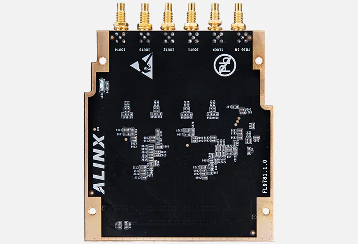
Description and Technical Data:
1) Overview/Key Features
The FL9781 is a 4-channel, 14-bit, 500 MSPS digital-to-analog converter FMC card. It uses 2 AD9781 converter devices and provides 4 AC-coupled analog outputs through SSMC connectors. The card uses a standard FMC LPC interface for connection to compatible FPGA carrier boards and is suitable for high-speed signal-generation, communications, instrumentation, and digital-signal-processing applications.
- 4-channel digital-to-analog conversion
- 14-bit resolution per channel
- 500 MSPS update rate
- 2 AD9781 converter devices
- 50 Ω output impedance
- Programmable full-scale output current from 8.66 mA to 31.66 mA
- 20 mA default full-scale output current
- Analog output range from -350 mV to +350 mV
- 4 SSMC analog output interfaces
- AC-coupled outputs
- External clock input
- External trigger or synchronization input
- SPI configuration interface
- LVDS digital interface levels at 1.8 V or 2.5 V
- Standard FMC LPC interface
- Operating temperature range from -40°C to +85°C
- 76 mm × 69 mm card form factor
NCNR non cancelable - non returnable product. B2B customers please contact Mirifica Industrial for volume quotes. Mirifica Industrial ships world-wide.
2) Tech Specs
| Specification | Detail |
|---|---|
| Card type | 4-channel digital-to-analog converter FMC card |
| Converter devices | 2 × AD9781 |
| Number of DA channels | 4 |
| Resolution | 14-bit |
| Update rate | 500 MSPS |
| Output impedance | 50 Ω |
| Full-scale output current | 8.66 mA to 31.66 mA programmable; 20 mA default |
| Analog output range | -350 mV to +350 mV |
| Analog output interface | 4 × SSMC |
| Output coupling | AC coupling |
| External clock | 1 input |
| External trigger | 1 input, 3.3 V LVCMOS or LVTTL |
| Digital input logic level | LVDS at 1.8 V or 2.5 V |
| Configuration interface | SPI |
| FMC interface | ANSI/VITA 57.1 LPC FMC |
| Operating temperature | -40°C to +85°C |
| Card dimensions | 76 mm × 69 mm |
3) Tech Support/Documents
Web available technical information usually covers the FL9781 4-channel digital-to-analog converter architecture, AD9781 converter devices, analog output channels, output current, output impedance, AC coupling, external clock and trigger inputs, SPI configuration, LVDS digital interface levels, FMC LPC connectivity, operating temperature, and card dimensions.
There are the following technical resources and development materials: a user manual, schematic documentation, demonstration projects where applicable, and connection information for compatible FPGA development boards with FMC interfaces.
Contact Mirifica Industrial for further detailed information for your project.
4) Related Product Suggestion
- AX7325 FPGA development board with compatible FMC connector J7
- AX7325B FPGA development board with compatible FMC connector J7
- AX7350 FPGA development board with compatible FMC connector J15
- AX7450 FPGA development board with compatible FMC connector J7
- AXKU040 FPGA development board with compatible FMC connector FMC2/J6
- AXKU041 FPGA development board with compatible FMC connector FMC2/J2
- AXKU042 FPGA development board with compatible FMC connector FMC2/J13
- AXU4EV-P FPGA development board with compatible FMC connector J41
- AXU5EV-P FPGA development board with compatible FMC connector J41
- AXU9EG FPGA development board with compatible FMC connector J7
- AXU15EG FPGA development board with compatible FMC connector J7
- Z7-P FPGA development board with compatible FMC connector J13
- Z19 FPGA development board with compatible FMC connector FMC2/J33
- Z19-P FPGA development board with compatible FMC connector FMC2/J19
5) Downloads/Links
6) What is in the package
The package contains.
- 1 x FL9781 FMC card
More Details:
FMC Cards