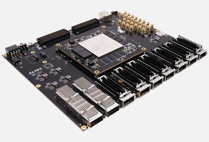
Description and Technical Data:
1) Overview/Key Features
The ALINX AXVU13G is a high-performance FPGA development and validation platform built around the XCVU13P Virtex UltraScale+ FPGA. It combines a removable ACVU13 system-on-module with a feature-rich carrier board for high-bandwidth data processing, network acceleration, hardware emulation, advanced communications, radar, test and measurement, and compute-intensive algorithm development.
Key features include:
- XCVU13P-2FHGB2104I Virtex UltraScale+ FPGA
- 3,780K system logic cells
- 12,288 DSP slices
- 76 GTY transceivers supporting data rates up to 28.21 Gbps
- Integrated 100G Ethernet MAC and 150G Interlaken cores
- 20 GB DDR4 SDRAM
- 2 x 128 MB QSPI flash memory
- 2 x QSFP-DD interfaces supporting up to 200 Gbps each
- 7 x QSFP28 interfaces supporting up to 100 Gbps each
- 1 x FMC+ expansion interface
- 1 x FMC HPC expansion interface
- 26 x SMA connectors for differential I/O, clock, trigger, and transceiver signals
- 1 x Gigabit Ethernet interface
- USB-to-UART interface
- MicroSD card interface
- JTAG programming and debugging interface
- 4 x LEDs, 1 x push-button, and 1 x DIP switch
- 12 V single-supply operation
- 210 mm x 255 mm board form factor
The platform is designed for applications including data-center acceleration, machine learning and AI, network processing, wired communications, 5G baseband, radar, test and measurement, emulation, and high-end FPGA prototyping.
NCNR non cancelable - non returnable product. B2B customers please contact Mirifica Industrial for volume quotes. Mirifica Industrial ships world-wide.
2) Tech Specs
| Specification | Detail |
|---|---|
| FPGA device | XCVU13P-2FHGB2104I |
| FPGA family | Virtex UltraScale+ |
| FPGA speed grade | -2 |
| FPGA temperature grade | Industrial |
| System logic cells | 3,780K |
| CLB flip-flops | 3,456K |
| CLB LUTs | 1,728K |
| Distributed RAM | 48.3 Mb |
| Block RAM | 94.5 Mb |
| UltraRAM | 360.0 Mb |
| DSP slices | 12,288 |
| Peak INT8 DSP performance | 38.3 TOP/s |
| PCIe Gen3 x16 capability | 4 |
| 150G Interlaken capability | 8 |
| 100G Ethernet with KR4 RS-FEC | 12 |
| GTY transceivers | 76, up to 28.21 Gbps |
| Maximum single-ended HP I/O | 702 |
| DDR4 SDRAM | 20 GB, 80-bit bus, 2,666 Mbps data rate |
| QSPI flash | 2 x 128 MB |
| QSFP-DD | 2 x 200G interfaces |
| QSFP28 | 7 x 100G interfaces |
| FMC+ | 1 interface, compatible with FMC+ and FMC |
| FMC HPC | 1 interface |
| Gigabit Ethernet | 1 x 10/100/1000M RJ45 interface |
| SMA interfaces | 26 total: 8 x RX, 8 x TX, 6 x CLK, 2 x MGT-CLK, 2 x TRIG |
| USB-to-UART | 1 interface |
| MicroSD | 1 slot, SD mode and SPI mode |
| JTAG | 14-pin, 2.00 mm standard interface |
| LEDs | 4 |
| Push-button | 1 reset button |
| DIP switch | 1 x 4-bit switch |
| Power input | +12 V DC through PCIe slot or PCIe 8-pin connector |
| Maximum input current | 15 A |
| Dimensions | 255 mm x 210 mm |
| PCB construction | Independent ground and power layers |
The XCVU13P device family provides substantial programmable logic, DSP, memory, I/O, and high-speed transceiver resources for high-throughput FPGA designs.
3) Tech Support/Dokuments
Web available technical information usually covers the ACVU13 system-on-module, carrier-board architecture, FPGA resources, memory configuration, high-speed optical interfaces, FMC expansion, SMA signal access, power input, programming interfaces, and supported development workflows. There are the following technical resources:
- AXVU13G user manual
- Hardware schematics
- Board interface documentation
- FPGA resource and pin information
- Reference designs
- Demonstration projects
- Development tutorials
- FPGA programming and debugging guidance
- Vivado design resources
- High-speed transceiver and networking references
Contact Mirifica Industrial for further detailed information for your project.
4) Related Product Suggestion
The ACVU13 system-on-module is available as a related product for designs that require the processing module separately from the AXVU13G carrier board. Compatible FMC and FMC+ expansion cards can also be used with the board’s expansion interfaces.
5) Downloads/Links
6) What is in the package
The package contains.
- 1 x system-on-module
- 1 x base board
- 1 x mini USB cable
- 1 x USB downloader cable set
- 1 x 12 V power adapter
- 1 x preinstalled heatsink kit
- 13 x SMA cables
- 1 x SD card
More Details:
FPGA Dev Boards