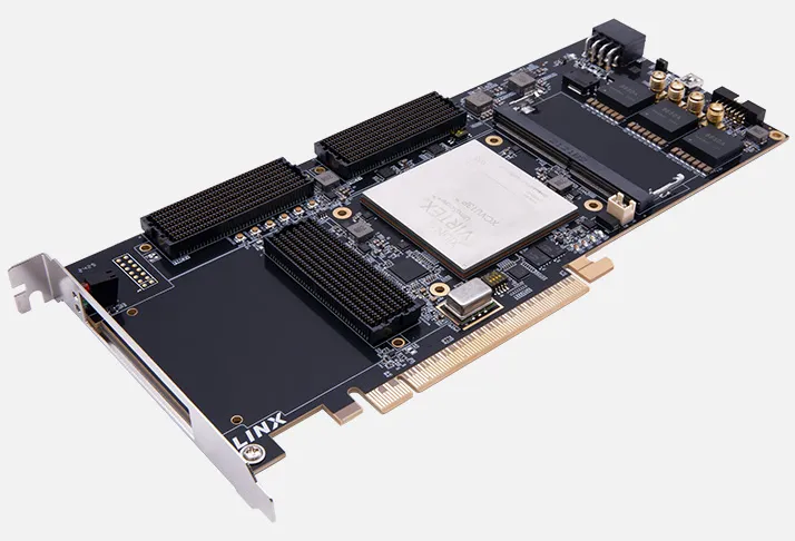
Description and Technical Data:
1) Overview/Key Features
The ALINX AXVU13P is a high-performance FPGA development board and design-in kit built around the AMD/Xilinx Virtex™ UltraScale+™ XCVU13P FPGA. It provides three FMC+ expansion interfaces for data acquisition, motor control, display, camera, software-defined radio and other high-speed application modules. The board also integrates PCIe Gen3 ×16, DDR4 SODIMM memory, high-speed GTY transceivers, QSPI Flash, UART and JTAG interfaces. Typical applications include compute acceleration, machine learning and AI, network acceleration, wired communications, 5G baseband, radar, test and measurement, emulation and prototyping.
Key features include:
- XCVU13P-2FHGB2104I Virtex UltraScale+ FPGA
- 16 nm FinFET FPGA fabric
- Integrated 100G Ethernet MAC and 150G Interlaken cores
- Integrated PCIe Gen3 ×16 block
- 32 Gigabit GTY transceivers
- Up to 38 TOPS and 22 TeraMACs of DSP compute performance
- Support for fixed-point, floating-point and INT8 AI inference workloads
- One DDR4 SODIMM slot supporting up to 16 GB DDR4
- Two 128 MB QSPI Flash devices
- Three FMC+ connectors
- 12 V single-supply operation
- 251 × 111.15 mm board form factor
NCNR non cancelable - non returnable product. B2B customers please contact Mirifica Industrial for volume quotes. Mirifica Industrial ships world-wide.
2) Tech Specs
| Specification | Detail |
|---|---|
| Product model | AXVU13P |
| Product type | FPGA development board and design-in kit |
| FPGA family | AMD/Xilinx Virtex UltraScale+ |
| FPGA device | XCVU13P-2FHGB2104I |
| FPGA process | 16 nm FinFET |
| FPGA package | FHGB2104 |
| GTY transceivers | 32 Gigabit GTY listed in the key features; product matrix lists 76 GTY resources |
| DSP performance | Up to 38 TOPS; up to 22 TeraMACs |
| AI support | INT8 inference, fixed-point and floating-point processing |
| DDR4 memory | 1 × DDR4 SODIMM slot, supports up to 16 GB |
| QSPI Flash | 2 × 128 MB |
| PCIe | 1 × PCIe Gen3 ×16 |
| FMC+ connectors | 3 |
| FMC+ 1 | 120 I/Os and 20 GTY |
| FMC+ 2 | 120 I/Os and 16 GTY |
| FMC+ 3 | 164 I/Os and 24 GTY |
| High-speed interfaces | FMC+, PCIe Gen3 ×16 and GTY transceivers |
| UART | 1 × USB-to-UART |
| JTAG | 1 |
| SMA | 2 |
| User indicators | 8 LEDs |
| User input | 1 key |
| Power input | 12 V single supply |
| Board dimensions | 251 × 111.15 mm |
3) Tech Support/Dokuments
Web available technical information usually covers the AXVU13P product description, FPGA device, key features, interface allocation, applications, product-selection information, package contents, documentation and related products. The AXVU13P V1.0 User Manual and further documentation and tutorials are available.
Contact Mirifica Industrial for further detailed information for your project.
4) Related Product Suggestion
Manufacturer-listed related products include:
- AXVU13F FPGA Dev Board & Kit with AMD Virtex US+ XCVU13P
- AXKU15 FPGA Dev Board & Kit with AMD Kintex™ US+ XCKU15P
- AXKU5 FPGA Dev Board & Kit with AMD Kintex™ US+ XCKU5P
- AXKU3 FPGA Dev Board & Kit with AMD Kintex™ US+ XCKU3P
- AXAU15 FPGA Dev Board & Kit with AMD Artix™ US+ XCAU15P
- AXVU13G FPGA Dev Board & Kit with AMD Virtex US+ XCVU13P
- AXVU9F FPGA Dev Board & Kit with AMD Virtex US+ XCVU9P
- AXVU9G FPGA Dev Board & Kit with AMD Virtex US+ XCVU9P
- HEA13 FPGA Dev Board & Kit with AMD Virtex US+ XCVU13P
- ACVU13 FPGA SoM with AMD Virtex US+ XCVU13P
5) Downloads/Links
6) What is in the package
The package contains.
- 1 × Development board
- 1 × FAN8060 heatsink kit, preinstalled
- 1 × Mini USB cable
- 1 × USB downloader cable/set
- 1 × 12 V power adapter
- 1 × PCIe fence
More Details:
FPGA Dev Boards