Description and Technical Data:
1) Overview/Key Features
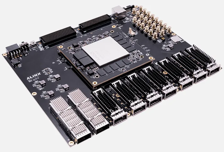
The ALINX AXVU9G is a high-performance FPGA development and validation platform based on the Virtex UltraScale+ XCVU9P FPGA. It combines a pluggable ACVU9 system-on-module with a high-speed carrier board, providing substantial programmable logic, DSP resources, high-speed GTY transceivers, QSFP-DD and QSFP28 networking, FMC expansion, and multiple debug interfaces.
- Virtex UltraScale+ XCVU9P FPGA installed on a pluggable ACVU9 system-on-module
- 2,586K system logic cells
- 6,840 DSP slices
- Peak INT8 DSP performance up to 38.3 TOPS
- 76 GTY transceivers supporting data rates up to 28.21 Gbps
- Integrated 100G Ethernet MAC and 150G Interlaken cores
- 20 GB DDR4 SDRAM
- 2 x 128 MB QSPI Flash
- 2 x QSFP-DD interfaces supporting up to 200 Gbps each
- 7 x QSFP28 interfaces supporting up to 100 Gbps each
- 1 x FMC+ interface and 1 x FMC HPC interface
- 11 x SMA pairs for high-speed transceivers, differential clocking, and triggering
- 1 x Gigabit Ethernet interface
- 1 x USB-to-UART interface
- 1 x MicroSD card interface
- 1 x JTAG interface
- 5 x user LEDs, 1 x push button, and 1 x DIP switch
- 12 V DC single-supply operation
- Suitable for AI acceleration, communications, radar, 5G baseband, network processing, emulation, test and measurement, and FPGA prototyping
NCNR non cancelable - non returnable product. B2B customers please contact Mirifica Industrial for volume quotes. Mirifica Industrial ships world-wide.
2) Tech Specs
| Specification | Detail |
|---|---|
| FPGA device | Virtex UltraScale+ XCVU9P-2FLGB2104 |
| System logic cells | 2,586K |
| DSP slices | 6,840 |
| Peak INT8 DSP performance | Up to 38.3 TOPS |
| GTY transceivers | 76 |
| GTY transceiver speed | Up to 28.21 Gbps |
| Integrated networking cores | 100G Ethernet MAC and 150G Interlaken cores |
| DDR4 SDRAM | 20 GB |
| QSPI Flash | 2 x 128 MB |
| QSFP-DD interfaces | 2 x QSFP-DD, up to 200 Gbps each |
| QSFP28 interfaces | 7 x QSFP28, up to 100 Gbps each |
| FMC expansion | 1 x FMC+ interface and 1 x FMC HPC interface |
| SMA interfaces | 11 pairs: 9 pairs connected to GTY transceivers, 1 differential-clock pair, and 1 trigger pair |
| Ethernet | 1 x Gigabit Ethernet |
| Serial interface | 1 x USB-to-UART interface |
| Storage interface | 1 x MicroSD card slot |
| Debug interface | 1 x JTAG interface |
| User controls | 5 x LEDs, 1 x push button, and 1 x DIP switch |
| Power input | 12 V DC single supply |
| Board dimensions | 210 x 255 mm |
3) Tech Support/Dokuments
Web available technical information usually covers the AXVU9G system-on-module and carrier-board architecture, the XCVU9P FPGA resources, DDR4 and QSPI memory, GTY transceivers, QSFP-DD and QSFP28 interfaces, FMC expansion, SMA connectivity, Ethernet, MicroSD, UART, JTAG, power input, and supported FPGA development applications.
There are the following technical resources available:
- AXVU9G V1.0 User Manual
- AXVU9G product information
- ACVU9 system-on-module information
- Hardware interface and connector information
- High-speed networking and transceiver information
- Development demos and tutorials
- Application information for AI, communications, radar, and data acceleration
Contact Mirifica Industrial for further detailed information for your project.
4) Related Product Suggestion
- ACVU9 system-on-module
- AXVU13G FPGA Development Board & Kit with Virtex UltraScale+ XCVU13P
- AXVU13F FPGA Development Board & Kit with Virtex UltraScale+ XCVU13P
- AXVU9F FPGA Development Board & Kit with Virtex UltraScale+ XCVU9P
5) Downloads/Links
6) What is in the package
The package contains.
- 1 x ACVU9 system-on-module
- 1 x Base Board
- 1 x Mini USB Cable
- 1 x USB Downloader Cable/Set
More Details:
FPGA Dev Boards