Description and Technical Data:
1) Overview/Key Features
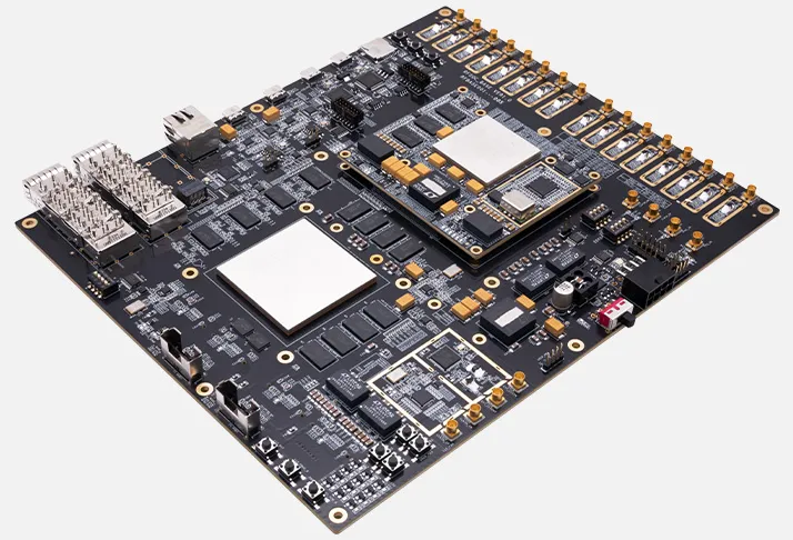
The ALINX AXW47 is a high-performance RFSoC development board based on the AMD Zynq UltraScale+ RFSoC Gen 3 XCZU47DR device. It combines programmable FPGA logic, an Arm processor subsystem, integrated high-speed RF data converters, and extensive high-bandwidth connectivity for advanced wireless, radar, satellite, instrumentation, and signal-processing applications. The carrier board also includes an XCKU115 pure-logic FPGA for backend processing acceleration.
Key features include:
- XCZU47DR Zynq UltraScale+ RFSoC Gen 3 device
- XCKU115 pure-logic FPGA for additional processing
- 8 x 14-bit RF ADC channels with sampling rates up to 5 GSPS
- 8 x 14-bit RF DAC channels with sampling rates up to 9.85 GSPS
- RF input and output interfaces supporting frequency bands up to 6 GHz
- 16 x 1 GB DDR4 SDRAM with a 64-bit data width
- 2 x 64 MB QSPI flash memory
- 2 x 40G QSFP+ fiber-optic interfaces
- 1 x 10G SFP+ fiber-optic interface
- 1 x Gigabit Ethernet interface
- 4 x M.2 interfaces
- 2 x MGB interfaces
- 2 x USB 3.0 interfaces
- 2 x USB/JTAG interfaces
- 1 x SD card interface
- User-defined status indicators and control keys
- 12 V single-supply operation
- 260 mm x 215 mm board form factor
NCNR non cancelable - non returnable product. B2B customers please contact Mirifica Industrial for volume quotes. Mirifica Industrial ships world-wide.
2) Tech Specs
| Specification | Detail |
|---|---|
| Primary device | XCZU47DR Zynq UltraScale+ RFSoC Gen 3 |
| Additional FPGA | XCKU115 pure-logic FPGA |
| RF ADCs | 8 channels, 14-bit, up to 5 GSPS |
| RF DACs | 8 channels, 14-bit, up to 9.85 GSPS |
| RF operating range | Interfaces designed for frequency bands up to 6 GHz |
| DDR4 memory | 16 x 1 GB devices, 64-bit data width |
| QSPI flash | 2 x 64 MB |
| 40G connectivity | 2 x QSFP+ fiber-optic interfaces |
| 10G connectivity | 1 x SFP+ fiber-optic interface |
| Ethernet | 1 x Gigabit Ethernet |
| M.2 interfaces | 4 |
| MGB interfaces | 2 |
| USB 3.0 | 2 interfaces |
| USB/JTAG | 2 interfaces |
| SD card | 1 interface |
| Status indicators | 4 fixed LEDs plus 8 user-defined LEDs |
| Control keys | 5 |
| Power input | 12 V single supply |
| Board dimensions | 260 mm x 215 mm |
The RF converter capabilities correspond to the Gen 3 RFSoC family, which supports up to 8 ADCs at 5.0 GSPS and DACs at up to 9.85 GSPS for operation up to approximately 6 GHz.
3) Tech Support/Dokuments
Web available technical information usually covers the board architecture, FPGA and RFSoC device capabilities, interface configuration, memory resources, power requirements, and development-tool compatibility. There are the following types of technical resources:
- Board user documentation
- Hardware specifications and interface descriptions
- FPGA and RFSoC development references
- Reference designs and example projects
- Vivado design resources
- RF data-converter configuration and evaluation tools
- RFSoC frequency-planning resources
- Embedded software and board-support resources
Contact Mirifica Industrial for further detailed information for your project.
4) Related Product Suggestion
The AXW47 is suitable for use with compatible M.2 storage or interface modules and external QSFP+ or SFP+ fiber-optic transceiver accessories. These accessories are not included in the standard package unless separately specified.
5) Downloads/Links
- Zynq UltraScale+ RFSoC Product Brief
- Zynq UltraScale+ RFSoC Frequency Planner
- RF Analyzer Downloads
- Adaptive SoCs & FPGA Embedded Software Downloads
6) What is in the package
The package contains.
- 1 x ALINX AXW47 development board
More Details:
FPGA Dev Boards