Description and Technical Data:
1) Overview/Key Features
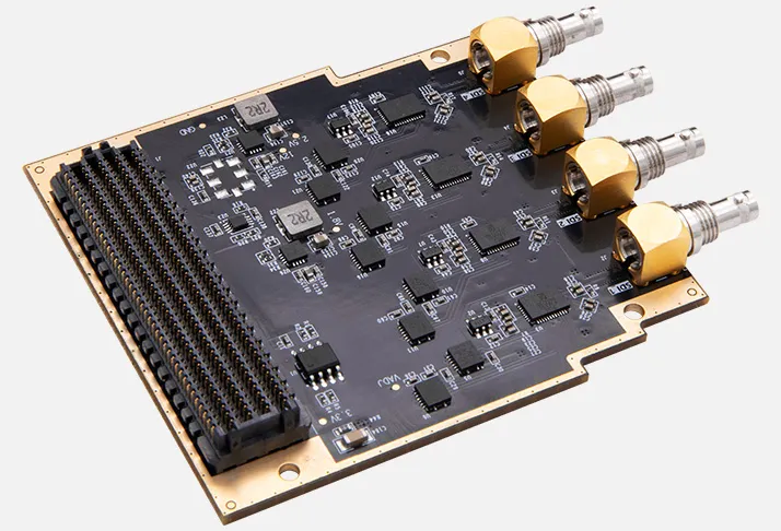
The ALINX FH1219 is a 4-channel bidirectional 12G-SDI 4K video input/output HPC FMC card. Each SDI channel can be configured independently as an input or output and supports SD, HD, 3G, 6G, and 12G-SDI signal rates. The card is designed for FPGA-based professional video processing, broadcast, image acquisition, video routing, and high-resolution video output applications.
- 4 x bidirectional 12G-SDI channels
- Each SDI channel can be configured independently for input or output
- Supports SD/HD/3G/6G/12G-SDI signal rates
- Supports video resolutions up to 4K at 60 frames per second
- 4 x HDBNC SDI connectors
- Maximum data rate of 11.88 Gbps per SDI channel
- FMC HPC interface compatible with the ANSI/VITA 57.1 FMC standard
- Uses the GS12190 bidirectional 12G-UHD-SDI device
- 75 Ω video signal impedance
- Reference clocks of 148.5 MHz and 148.35 MHz
- Industrial operating temperature range from -40 °C to 85 °C
- Compact 76.5 x 69 mm form factor
NCNR non cancelable - non returnable product. B2B customers please contact Mirifica Industrial for volume quotes. Mirifica Industrial ships world-wide.
2) Tech Specs
| Specification | Detail |
|---|---|
| Product type | 4-channel bidirectional 12G-SDI HPC FMC card |
| SDI channels | 4 |
| SDI direction | Each channel independently configurable as input or output |
| Supported SDI standards | SD, HD, 3G-SDI, 6G-SDI, and 12G-SDI |
| Maximum SDI data rate | 11.88 Gbps per channel |
| Maximum video capability | 4K video at 60 frames per second |
| SDI connectors | 4 x HDBNC |
| Video impedance | 75 Ω |
| SDI device | GS12190 bidirectional 12G-UHD-SDI device |
| FMC interface | FMC HPC interface compatible with ANSI/VITA 57.1 |
| Reference clocks | 148.5 MHz and 148.35 MHz |
| Operating temperature | -40 °C to 85 °C |
| Dimensions | 76.5 x 69 mm |
3) Tech Support/Dokuments
Web available technical information usually covers the FH1219 4-channel bidirectional 12G-SDI architecture, supported SDI standards, FMC HPC interface, HDBNC connections, reference-clock inputs, operating temperature range, and integration with compatible FPGA carrier boards. There are the following technical resources listed for this product:
- FH1219 V1.0 User Manual
- FH1219 Schematic diagram
Contact Mirifica Industrial for further detailed information for your project.
4) Related Product Suggestion
Compatible related FPGA development platforms listed for the FH1219 include:
- Z19 Dev Board & Kit with AMD Zynq™ UltraScale+™ MPSoC XCZU19EG
- Z19-P Dev Board & Kit with AMD Zynq™ UltraScale+™ MPSoC XCZU19EG
- AXU15EGB Dev Board & Kit with AMD Zynq™ UltraScale+™ MPSoC ZU15EG
- Z7-P Dev Board & Kit with AMD Zynq™ UltraScale+™ MPSoC XCZU7EV
- AXU5EVB-P Dev Board & Kit with AMD Zynq™ UltraScale+™ MPSoC ZU5EV
- AX7450B Dev Board & Kit with AMD Zynq™ 7000 SoC XC7Z100
- AX7350B Dev Board & Kit with AMD Zynq™ 7000 SoC XC7Z035
- AXKU15 FPGA Dev Board & Kit with AMD Kintex™ UltraScale+™ XCKU15P
- AXKU5 FPGA Dev Board & Kit with AMD Kintex™ UltraScale+™ XCKU5P
- AXAU15 FPGA Dev Board & Kit with AMD Artix™ UltraScale+™ XCAU15P
- AXKU062 FPGA Dev Board & Kit with AMD Kintex UltraScale™ XCKU060
- AXKU040 FPGA Dev Board & Kit with AMD Kintex UltraScale™ XCKU040
- AXKU041 FPGA Dev Board & Kit with AMD Kintex UltraScale™ XCKU040
- AX7325B FPGA Dev Board & Kit with AMD Kintex™ 7 XC7K325T
5) Downloads/Links
6) What is in the package
The package contains.
- 1 x FMC Card
More Details:
FMC Cards