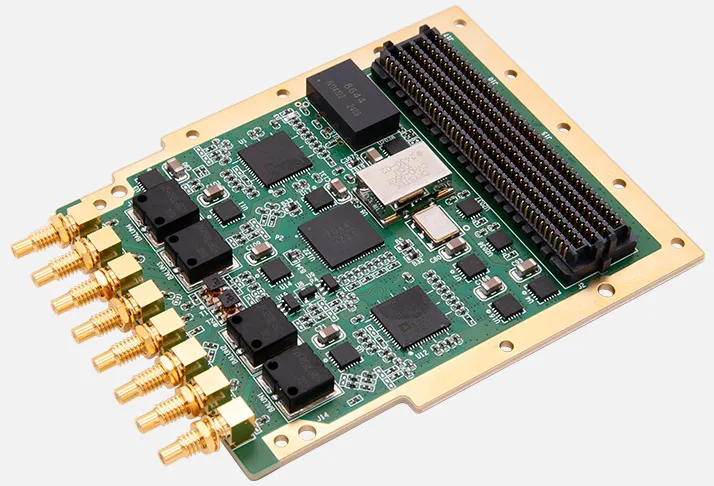
Description and Technical Data:
1) Overview/Key Features
The FH9681 is a VITA 57.1-compliant FMC analog-to-digital converter card with a JESD204B Subclass 1 interface. It provides 4-channel, 14-bit analog acquisition at a fixed sampling rate of 1 GSPS and is designed for use with compatible FPGA carrier boards featuring high-speed serial transceivers.
The card uses a GMS011 ADC device compatible with the AD9680-1000 architecture. It provides a full-power analog input bandwidth of up to 2 GHz, DC-coupled inputs, 8 high-speed serial GTX transceiver connections, and a 2 Vpp analog input range. The FH9681 is suitable for radar, smart antennas, wireless infrastructure, broadband RF signal processing, communication test equipment, millimeter-wave communication, autonomous-driving radar, and signal-generation applications.
- 4-channel, 14-bit ADC acquisition
- 1 GSPS sampling rate per channel
- JESD204B Subclass 1 digital interface
- 8 high-speed serial GTX transceiver connections
- Up to 10 Gbps maximum JESD204B lane rate
- 2 GHz full-power analog input bandwidth at -3 dB
- DC-coupled analog inputs from DC to 2 GHz
- 2 Vpp analog input range
- HMC7044 high-performance clock generator
- External reference-clock or external VCO-clock input
- LVTTL trigger input and trigger output
- VITA 57.1 FMC form factor
NCNR non cancelable - non returnable product. B2B customers please contact Mirifica Industrial for volume quotes. Mirifica Industrial ships world-wide.
2) Tech Specs
| Specification | Detail |
|---|---|
| Module type | FMC analog-to-digital converter card |
| FMC standard | VITA 57.1 |
| ADC resolution | 14 bit |
| ADC channels | 4 |
| Sampling rate | 1 GSPS per channel |
| Digital interface | JESD204B Subclass 1 |
| JESD204B lane configuration | Mixed lane configuration, maximum lane rate 10 Gbps |
| FPGA transceiver connection | 8 high-speed GTX transceiver connections |
| ADC device | GMS011 |
| Analog input coupling | DC-coupled |
| Analog input bandwidth | DC to 2 GHz; full-power bandwidth of 2 GHz at -3 dB |
| Analog input amplitude | 2 Vpp |
| Signal-to-noise ratio | 65 dBFS at 170 MHz input frequency and -1 dBFS amplitude |
| Spurious-free dynamic range | 82 dBFS at 170 MHz input frequency and -1 dBFS amplitude |
| Effective number of bits | 10.7 bit at 170 MHz input frequency and -1 dBFS amplitude |
| ADC power consumption | 1.65 W per channel at 1 GSPS |
| Clock generator | HMC7044 |
| Local oscillator | 100 MHz VCXO |
| External clock input | 1 x external reference-clock or external VCO-clock input |
| Trigger input | 1 x LVTTL trigger input, +3.3 V level |
| Trigger output | 1 x LVTTL trigger output, +3.3 V level |
| Typical power consumption | 8 W |
| Power supply | +12 V from the carrier board |
| Cooling | Natural air convection |
| Board dimensions | 84.1 x 69 mm |
| Operating temperature | -40 °C to +85 °C |
| Storage temperature | -55 °C to +125 °C |
| Operating humidity | 5% to 95%, non-condensing |
3) Tech Support/Documents
Web available technical information usually covers the FH9681 FMC architecture, JESD204B Subclass 1 interface, ADC performance, clock generation, trigger operation, analog input characteristics, FPGA transceiver connectivity, power requirements, environmental limits, and supported RF and communications applications. There are the following technical resources:
- FH9681 product information
- Module features and functional block diagram
- ADC performance specifications
- JESD204B interface information
- Clock and trigger configuration information
- FMC mechanical and electrical specifications
- Applications guidance for radar, wireless infrastructure, communications testing, and autonomous-driving radar
- User manual availability through the product documentation area
Contact Mirifica Industrial for further detailed information for your project.
4) Related Product Suggestion
No additional add-on products are specified on the product page.
5) Downloads/Links
6) What is in the package
The package contains.
- 1 x FH9681 FMC card
More Details:
FMC Cards