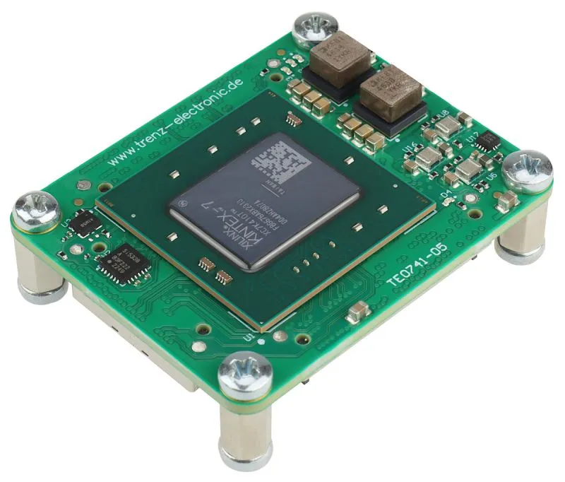
Description and Technical Data:
1) Overview/Key Features
The TE0741-05-G2C-1-A is a compact 4 × 5 cm FPGA module based on the AMD Kintex™-7 XC7K410T-2FBG676C FPGA. It is designed for high-performance embedded processing, digital signal processing, communications, industrial control, instrumentation, and custom FPGA applications.
Key features include:
- AMD Kintex™-7 XC7K410T FPGA
- XC7K410T-2FBG676C device
- 32 MByte Quad-SPI flash memory for FPGA configuration and user data
- 8 MGT multi-gigabit transceivers
- Up to 144 FPGA I/O signals available through board-to-board connectors
- Up to 65 LVDS pairs, depending on the selected interface configuration
- JTAG and SPI configuration options
- 25 MHz low-jitter oscillator with shutdown control
- Programmable Silicon Labs Si5338 quad-clock generator
- High-performance on-board DC-DC converters
- Dedicated MGT voltage regulation
- Core voltage regulator rated up to 30 A, depending on the module variant
- 2 × 100-pin and 1 × 60-pin high-speed Razor Beam board-to-board connectors
- 2 user LEDs and 1 FPGA DONE indicator
- AES bitstream encryption support
- Evenly distributed power pins for improved signal integrity
- Compact plug-on module design
- Mechanical compatibility with other 4 × 5 cm modules in the same product family
The module is intended for use with a compatible carrier board. All components cover at least the commercial temperature range of 0 °C to +70 °C; the usable module temperature depends on the customer design, operating conditions, and selected cooling solution.
NCNR non cancelable - non returnable product. B2B customers please contact Mirifica Industrial for volume quotes. Mirifica Industrial ships world-wide.
2) Tech Specs
| Specification | Detail |
|---|---|
| FPGA family | AMD Kintex™-7 |
| FPGA device | XC7K410T-2FBG676C |
| FPGA architecture | 7 Series |
| FPGA type | Programmable logic FPGA |
| Speed grade | -2 |
| Temperature grade | Commercial |
| Package | FBG676 |
| Form factor | 4 × 5 cm |
| Configuration memory | 256 Mbit / 32 MByte Quad-SPI flash |
| Flash usage | FPGA configuration and user data storage |
| FPGA configuration interfaces | JTAG and SPI flash |
| Multi-gigabit transceivers | 8 MGTs |
| Available FPGA I/O | Up to 144 I/O pins through board-to-board connectors |
| Differential interfaces | Up to 65 LVDS pairs, depending on pin allocation |
| Main oscillator | 25 MHz low-jitter oscillator |
| Oscillator control | Shutdown control available |
| Clock generator | Silicon Labs Si5338 programmable quad-clock generator |
| Board-to-board connectors | 2 × 100-pin and 1 × 60-pin Razor Beam connectors |
| Connector type | High-speed hermaphroditic board-to-board connector |
| Connector pitch | 4 mm |
| Core power regulation | High-performance regulator rated up to 30 A, variant-dependent |
| MGT power regulation | Dedicated on-board MGT voltage regulator |
| Supply input | 3.3 V, or 3.3 V and 5 V depending on configuration |
| Status indicators | 2 user LEDs and 1 FPGA DONE indicator |
| Security feature | AES bitstream encryption support |
| Power distribution | Evenly distributed supply pins for improved signal integrity |
| Operating temperature reference | Components specified for at least 0 °C to +70 °C |
| Cooling requirement | Application-dependent and dependent on customer design |
The actual number of usable I/O pins, LVDS pairs, power requirements, and thermal performance depend on the carrier-board design and the implemented FPGA application.
3) Tech Support/Dokuments
Web available technical information usually covers the TE0741 Wiki documentation, design-support files, reference designs with source code, FPGA configuration methods, clock-generator examples, carrier-board information, and general interface documentation.
There are the following technical resources available for development:
- TE0741 Wiki documentation
- Reference designs with source code and configuration files
- TE0741 test-board examples
- Silicon Labs Si5338 reconfiguration examples
- Reference-design documentation for supported Vivado versions
- FPGA configuration information for JTAG and Quad-SPI flash
- Board-to-board connector and compatibility information
- Support forum assistance
- Vivado Enterprise Edition development-flow information
Contact Mirifica Industrial for further detailed information for your project.
4) Related Product Suggestion
Available add-on products and related hardware include:
- Compatible 4 × 5 cm carrier boards
- TE0741 test board
- Carrier boards for evaluating the module’s FPGA interfaces and clocking functions
- High-speed Razor Beam connector solutions for compatible carrier-board designs
The TE0741 test board is the most directly related development accessory for evaluation and reference-design work.
5) Downloads/Links
- Trenz Electronic TE0741 Wiki
- TE0741 test board reference design documentation
- TE0741 product page
- Support Forum
6) What is in the package
The package contains.
- 1 x TE0741-05-G2C-1-A 4 × 5 cm FPGA module with AMD Kintex™-7 XC7K410T FPGA
- 8 x screws
- 4 x spacer bolts