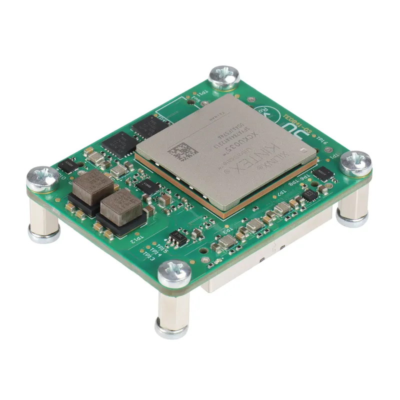
Description and Technical Data:
1) Overview/Key Features
The TE0841-03-31C31-A is a compact 4 × 5 cm FPGA micromodule based on the AMD Kintex™ UltraScale™ KU035. It combines programmable logic, 2 GByte DDR4 SDRAM, configuration flash, clock generation, power management, and high-speed I/O in a small module suitable for embedded, industrial, instrumentation, communications, and custom carrier-board applications.
- AMD Kintex™ UltraScale™ XCKU035-1SFVA784C FPGA
- 2 GByte DDR4 SDRAM with a 32-bit memory interface
- 64 MByte SPI boot flash
- Compact 40 × 50 mm form factor
- Rugged construction suitable for industrial applications
- 260 board-to-board terminals through 3 high-speed connector strips
- 60 HR I/O lines and 84 HP I/O lines
- 8 GTH serial-transceiver lanes
- 2 external MGT clock inputs
- Si5338 4-output PLL clock generator
- 200 MHz LVDS oscillator
- On-board power supplies with single-supply operation
- User-defined I/O-bank power
- Evenly distributed supply pins to support signal integrity
- 3 mm mounting holes for a compatible heat spreader
- Mechanical and largely electrical compatibility with other 4 × 5 cm modules
NCNR non cancelable - non returnable product. B2B customers please contact Mirifica Industrial for volume quotes. Mirifica Industrial ships world-wide.
2) Tech Specs
| Specification | Detail |
|---|---|
| FPGA device | AMD Kintex™ UltraScale™ XCKU035-1SFVA784C |
| FPGA family | Kintex UltraScale |
| FPGA package | SFVA784 |
| FPGA speed grade | -1 |
| FPGA temperature grade | Commercial, 0 °C to +70 °C component range |
| DDR4 SDRAM | 2 GByte, arranged as 2 banks of 1024 MByte |
| DDR4 interface | 32-bit total; each memory device uses a separate 16-bit interface |
| SPI boot flash | 64 MByte, 512 Mbit |
| Module dimensions | 40 × 50 mm |
| Mounting holes | 3 mm holes for a compatible heat spreader |
| Board-to-board connectors | 3 × high-speed hermaphroditic connector strips, regular 4 mm |
| Total connector terminals | 260 |
| HR I/O | 60 |
| HP I/O | 84 |
| GTH serial transceivers | 8 lanes |
| MGT external clock inputs | 2 |
| PLL clock generator | Si5338, 4 outputs |
| System oscillator | 200 MHz LVDS |
| Power input | Single-supply operation supported |
| I/O-bank power | User-defined |
| Operating-temperature note | Module operating temperature depends on the customer design and cooling solution |
3) Tech Support/Documents
Web available technical information usually covers the TE0841 module, connector compatibility, mechanical integration, memory and configuration interfaces, clocking, power architecture, reference designs, and development software. There are the following technical resources:
- TE0841 module documentation
- Hardware design support files
- Reference designs with source files
- Mechanical and connector integration information
- Base-board compatibility information
- Samtec high-speed connector documentation
- Vivado Enterprise Edition development support
- Technical support forum resources
Contact Mirifica Industrial for further detailed information for your project.
4) Related Product Suggestion
- Compatible 4 × 5 cm base boards for module evaluation and application development
- Compatible skyline heat spreader for thermal management
5) Downloads/Links
6) What is in the package
The package contains.
- 1 x TE0841-03-31C31-A 4 × 5 cm FPGA module with AMD Kintex™ UltraScale™ XCKU035
- 8 x screws
- 4 x bolts