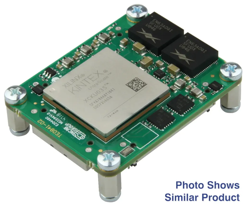
Description and Technical Data:
1) Overview/Key Features
The TE0841-03-32I31-A is a compact FPGA micromodule based on the AMD Kintex™ UltraScale™ KU035-2. It integrates 2 GByte of DDR4 SDRAM, 64 MByte of QSPI boot flash, onboard power supplies, programmable clocking, and high-speed configurable I/O in a rugged 40 mm × 50 mm form factor.
The module is designed for industrial embedded processing, high-performance FPGA computing, signal processing, communications, instrumentation, and custom hardware systems. Its 4 × 5 cm format is mechanically and largely electrically compatible with other modules in the same product family.
Key features include:
- AMD Kintex™ UltraScale™ XCKU035-2SFVA784I FPGA
- Industrial temperature-grade device
- Compact 40 mm × 50 mm form factor
- 2 GByte DDR4 SDRAM
- 32-bit DDR4 memory interface
- 64 MByte QSPI boot flash
- 260 rugged board-to-board terminals
- 60 × HR I/Os
- 84 × HP I/Os
- 8 × GTH serial transceiver lanes
- 2 × external MGT clock inputs
- Si5338 programmable clock generator
- 4-output PLL clocking
- 200 MHz LVDS oscillator
- Onboard power supplies
- Single-supply operation
- User-defined I/O-bank power
- 3 mm mounting holes for a Skyline heat spreader
- Evenly distributed supply pins for improved signal integrity
NCNR non cancelable - non returnable product. B2B customers please contact Mirifica Industrial for volume quotes. Mirifica Industrial ships world-wide.
2) Tech Specs
| Specification | Detail |
|---|---|
| Module type | FPGA micromodule |
| FPGA family | Kintex™ UltraScale™ |
| FPGA device | XCKU035-2SFVA784I |
| FPGA speed grade | -2 |
| FPGA package | SFVA784 |
| Temperature range | Industrial, -40 °C to +85 °C |
| Module dimensions | 40 mm × 50 mm |
| Form factor | 4 × 5 cm |
| DDR4 memory | 2 GByte |
| DDR4 organization | 2 banks of 1024 MByte |
| DDR4 interface | 32-bit total; each memory device uses a separate 16-bit interface |
| QSPI boot flash | 64 MByte / 512 Mbit |
| Board-to-board connectors | 3 × rugged high-speed hermaphroditic terminal/socket strips |
| Connector pitch | 4 mm |
| Total connector terminals | 260 |
| HR I/O | 60 |
| HP I/O | 84 |
| Serial transceivers | 8 × GTH lanes, TX/RX |
| External MGT clock inputs | 2 |
| Clock generator | Si5338, 4-output PLL |
| System oscillator | 200 MHz LVDS |
| Power architecture | Onboard switch-mode power supplies |
| Supply operation | Single-supply operation supported |
| User-defined power | User-defined I/O-bank power |
| Mounting holes | 3 mm holes for Skyline heat spreader |
| Power distribution | Evenly spread supply pins for improved signal integrity |
3) Tech Support/Documents
Web available technical information usually covers the FPGA device, memory architecture, boot flash, connector configuration, I/O resources, transceiver interfaces, clocking, power architecture, dimensions, and mechanical mounting provisions. There are the following technical support resources: compatible base boards, technical documentation, design support files, reference designs with source files, recommended FPGA development software, product-family compatibility information, and support forum access.
Contact Mirifica Industrial for further detailed information for your project.
4) Related Product Suggestion
- Compatible 4 × 5 cm module base boards
- Skyline heat spreader for mechanical mounting and thermal management
- High-speed board-to-board connector mating components for the Razor Beam interface
5) Downloads/Links
6) What is in the package
The package contains.
- 1 x TE0841-03-32I31-A 4 × 5 cm FPGA module with AMD Kintex™ UltraScale™ XCKU035
- 8 x screws
- 4 x bolts